GPS Golf Range Finder
Charlie Lindberg · 2024–2025
PCB and software by Charlie Lindberg; mechanical enclosure by Sam Handel
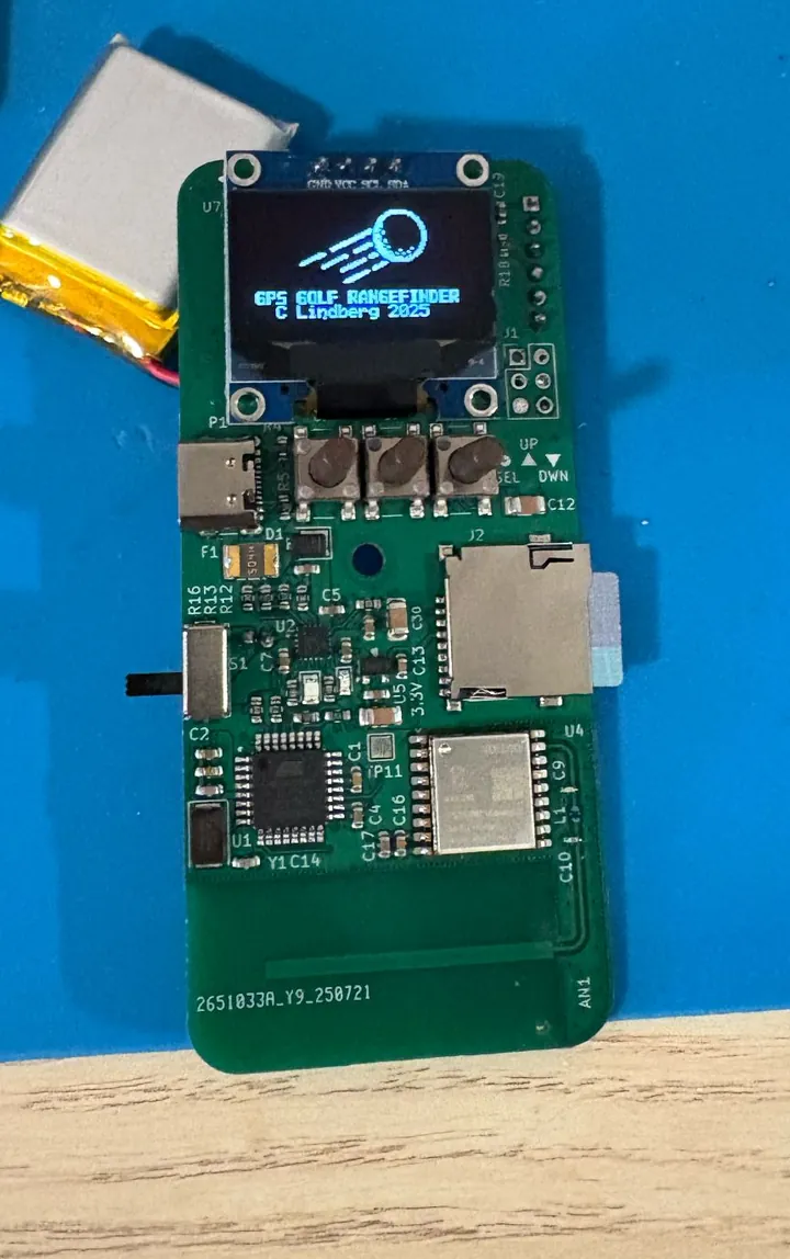
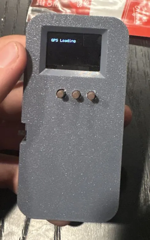
Overview
This is a GPS-based golf range finder that I designed and built: a custom PCB with an integrated PCB GPS antenna, an ATmega328P microcontroller, a small OLED screen, a microSD card holding course data, three buttons and a rechargeable LiPo battery. It shows the distance from where you are standing to the center of the green on the current hole. I was responsible for the PCB and software, and Sam Handel designed the mechanical enclosure.
I started this project in early 2024 because I wanted a simple, cheap and convenient way to get golf distances on the course.
Requirements
The goal was an ultra-low-cost golf range finder that gives accurate distances to the center of the green, is compact, has long battery life, and has an easy-to-read display and user interface. The three key design goals were:
| Goal | Target |
|---|---|
| Cost | < $25 |
| Accuracy | < 5 yards |
| Battery life | 8 hours minimum (two rounds of golf) |
System architecture
The device needs to acquire its distance to the green, store course data, display information to the user and take inputs. I chose GPS to acquire distance because it offered the lowest cost and high accuracy, an OLED screen to display data, and an SD card to store course information.
Component selection
- GPS receiver. I started with the GPS receiver, which was difficult to source. I selected a Vollgo GNSS module (VG7669T160N0SA), which outputs data over UART using the NMEA 0183 spec.
- Antenna. I designed a PCB GPS antenna to save size and cost (more below).
- Display. An OLED module with an SSD1306 driver, chosen for its size and ease of assembly. It connects over I2C.
- Storage. A basic microSD card receptacle on SPI.
- User interface. Three push buttons on GPIOs, polled in software with a time-based debounce.
That set the minimum interfaces the microcontroller needed: one I2C, one SPI, two UARTs (GPS and debug) and three GPIOs. I looked for the simplest MCU that could meet those needs and selected the ATmega328P for its low cost, low power consumption, and existing SSD1306 and microSD card libraries. It runs at 3.3 V and 8 MHz; the clock could probably come down to reduce power consumption.
PCB GPS antenna
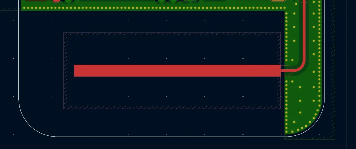
The antenna needs to operate in the GPS L1 band (1575.42 MHz). I looked at patch, quarter-wave (¼ λ) and bent quarter-wave antenna structures, and selected a straight ¼ λ antenna for the best performance, small size and a more omnidirectional radiation pattern.
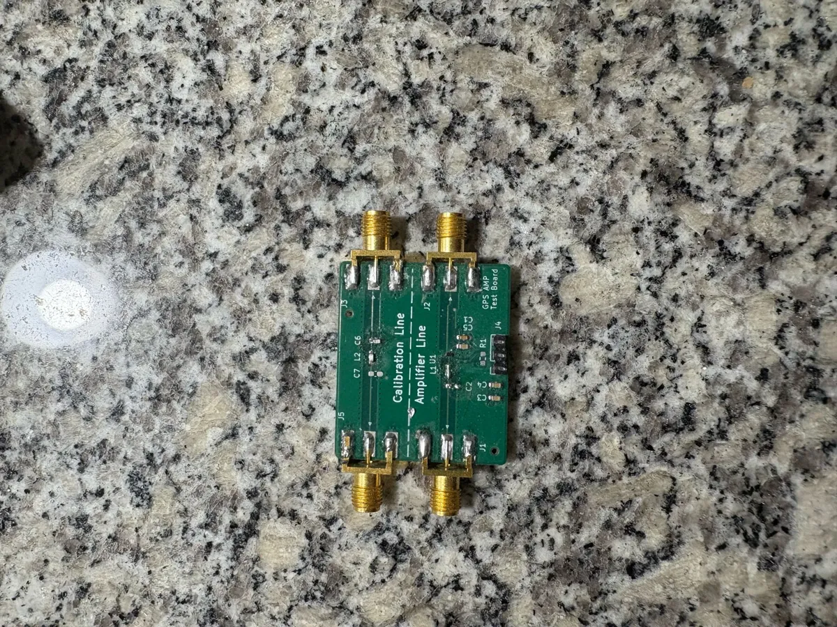
I calculated the quarter wavelength from the effective relative permittivity of a microstrip structure (λ = c / (f·√εeff)), then added 20% of additional length on a coupon board so the antenna could be tuned experimentally. Copper is voided on all layers below the antenna, and vias and planes form a ground plane at the base near the feed point.
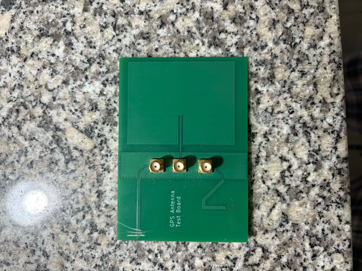
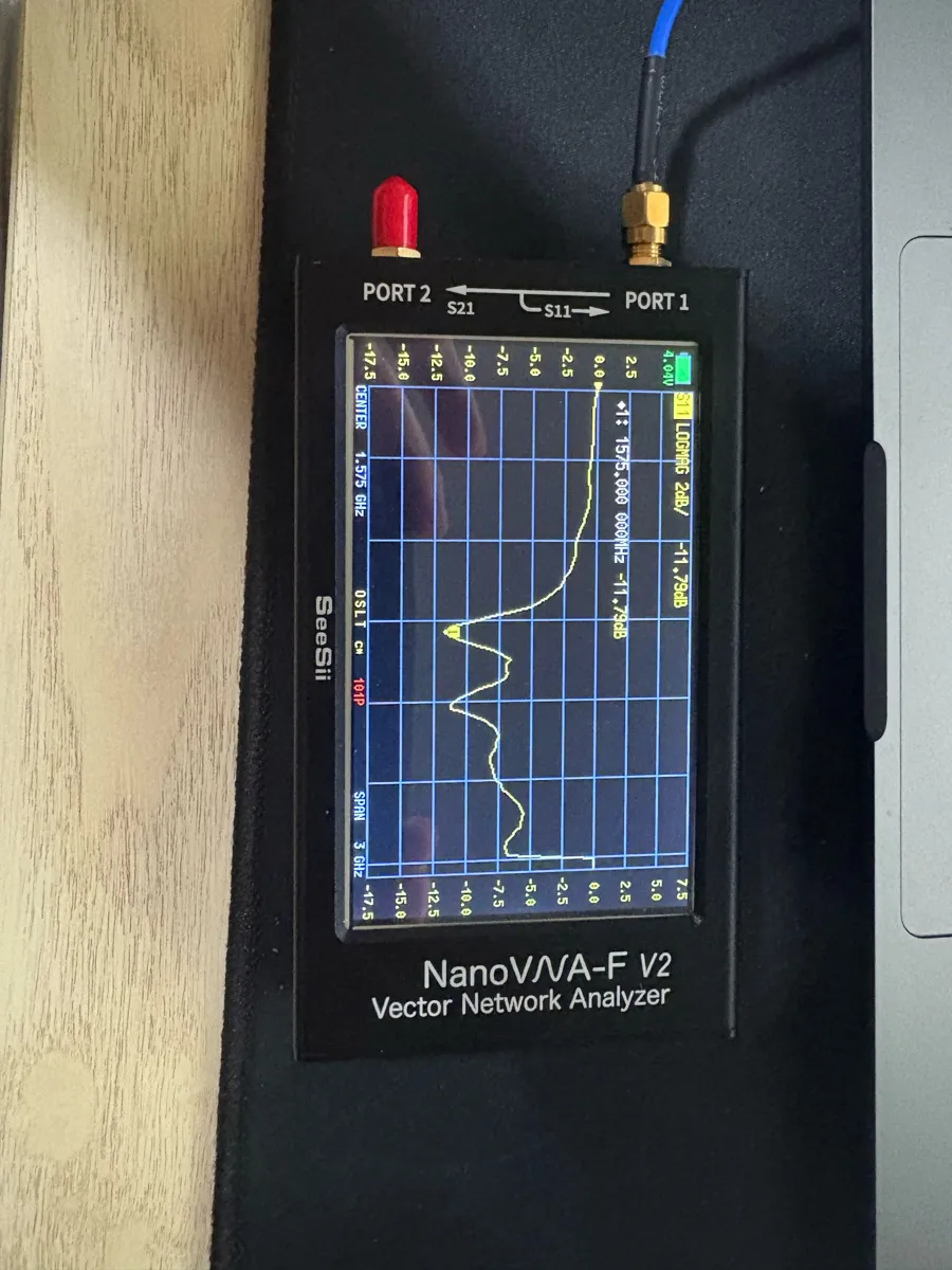
To tune it, I measured the S11 (input reflection) minimum, which started at lower frequencies, and successively trimmed the antenna until the minimum reached the center of the GPS L1 band. The final antenna showed a clear resonance at 1.575 GHz with an S11 of −11.8 dB, exceeding my initial target of −10 dB.
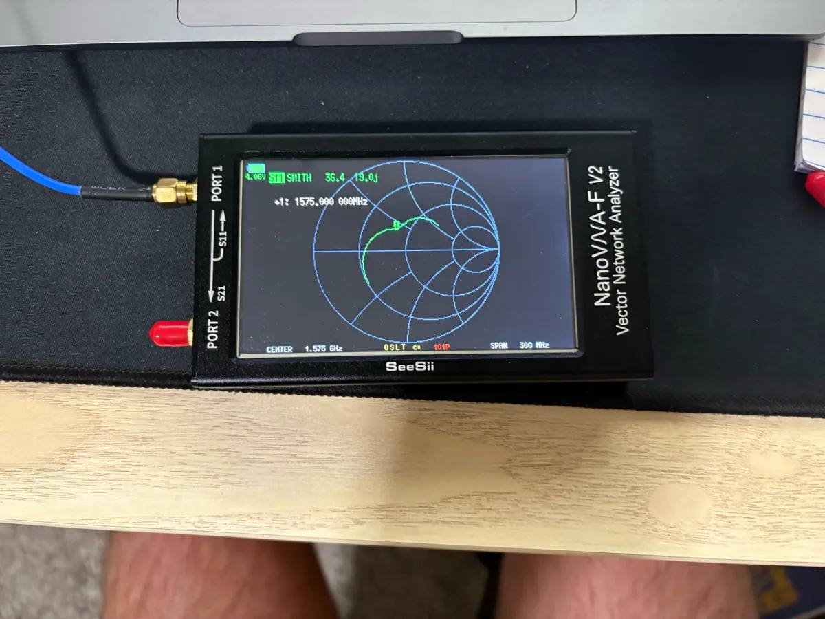
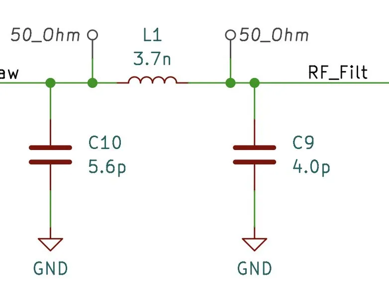
I measured the antenna's input impedance at 36 + 19j Ω at 1.575 GHz, so it needed to be matched to 50 Ω to maximize power transfer. Only about 15 MHz of bandwidth is needed, so a relatively high Q-factor is fine. I chose a C-L-C pi network for maximum flexibility; in the Rev 2 schematic it is 5.6 pF, 3.7 nH and 4.0 pF.
Rev 1
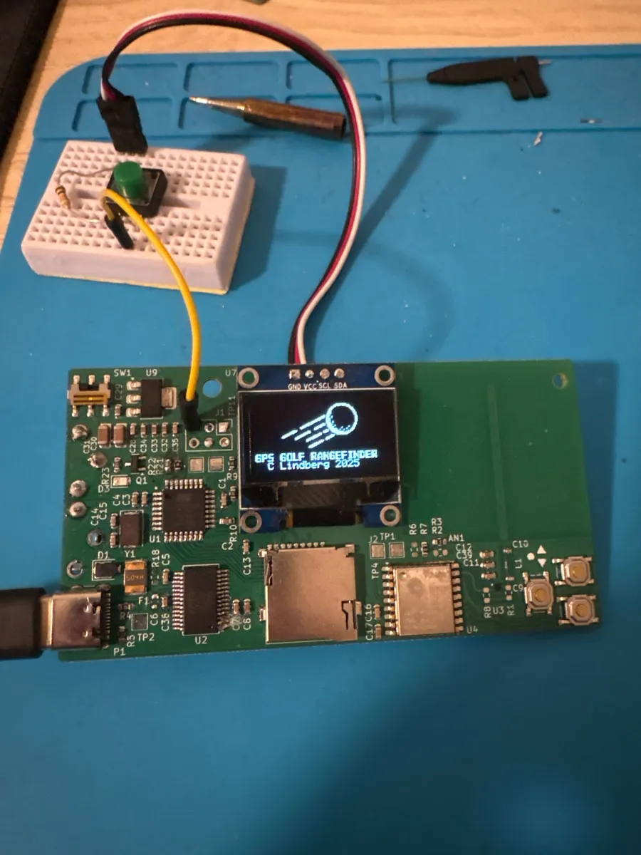
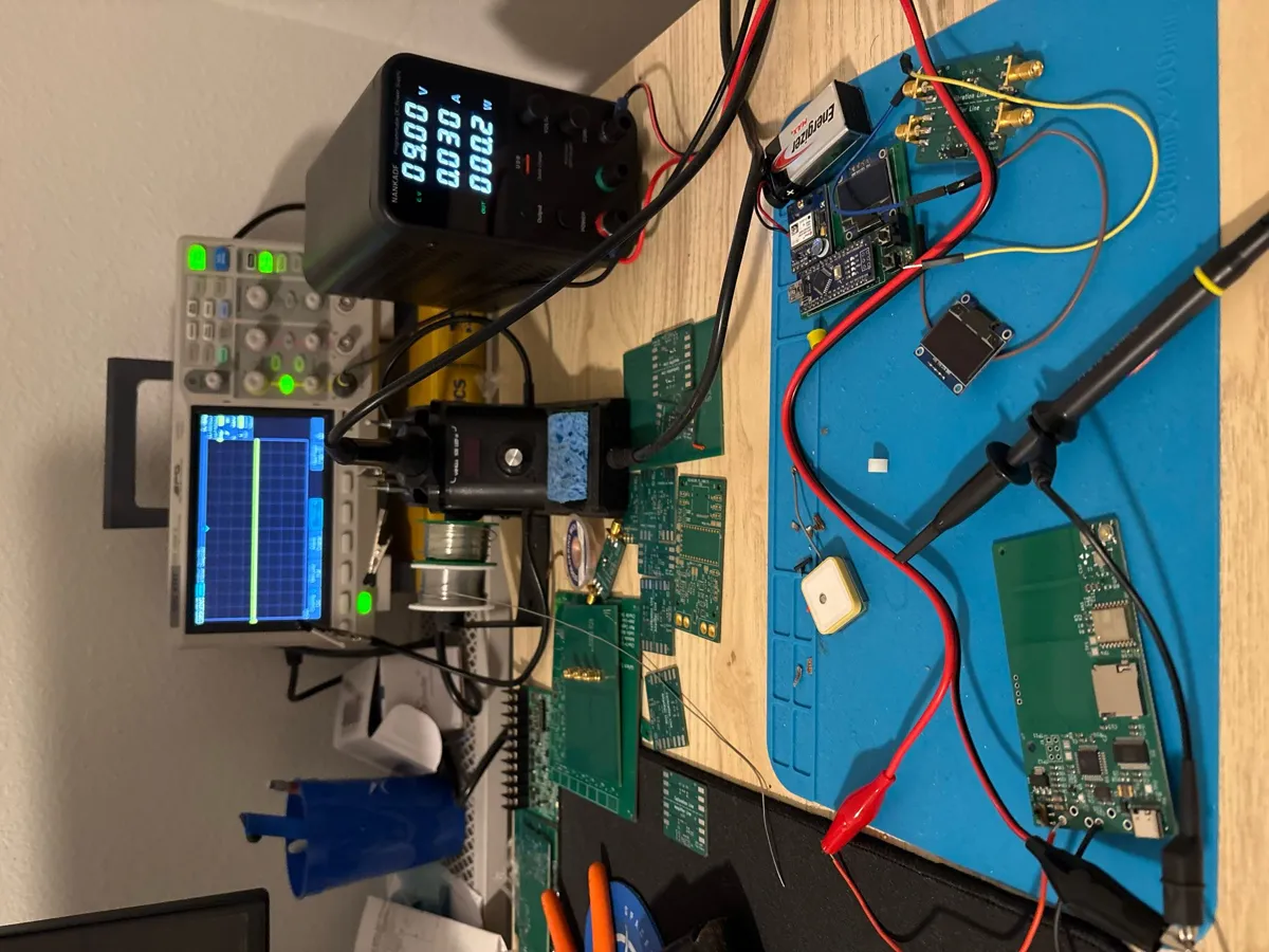
Rev 1 was designed to bring all of the systems onto a single board so I could begin writing software. I added a USB–UART interface to ease debugging and programming. I deliberately chose clunky mechanicals and a non-rechargeable battery to speed up development and de-risk the GPS functionality. Rev 1 was designed in January 2025, and I ordered the assembled boards from JLCPCB in March 2025.
Bring-up and debug:
- The initial smoke test passed and the 3.3 V rail behaved as expected.
- I had extended difficulty loading the bootloader onto the target MCU, which I tracked down to an improper configuration on the programmer MCU.
- The SD card and OLED screen behaved as expected.
- The GPS initially performed terribly, taking more than two minutes to get valid data. After comparing the performance and design to the coupons, I believe the cause was a matching inductor with a low self-resonant frequency, so I swapped to a wire-wound inductor for the next revision.
Rev 2
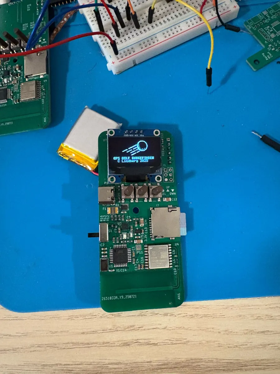
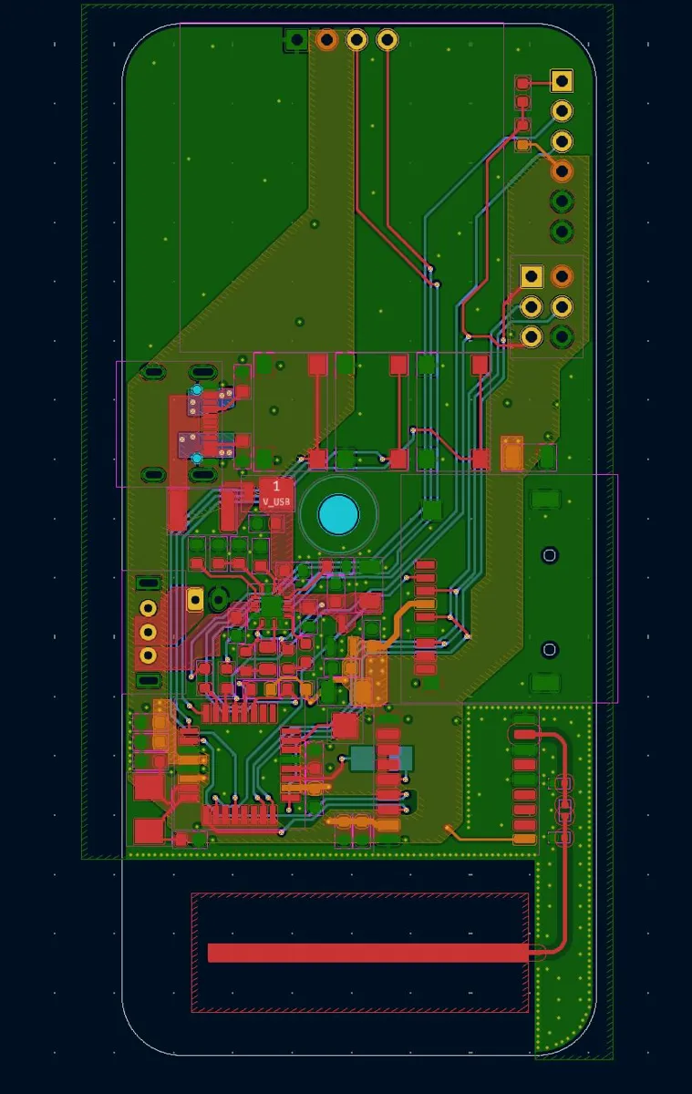
Rev 2 was designed in July 2025, and I ordered the assembled boards from JLCPCB later that month. The goals for Rev 2 were to improve the mechanicals, add a rechargeable battery, and delete components from Rev 1. I removed the USB–serial interface, the GPS amplifier and the large battery headers, downsized the LDO, and shrank the layout as much as possible. View the Rev 2 schematic (PDF).
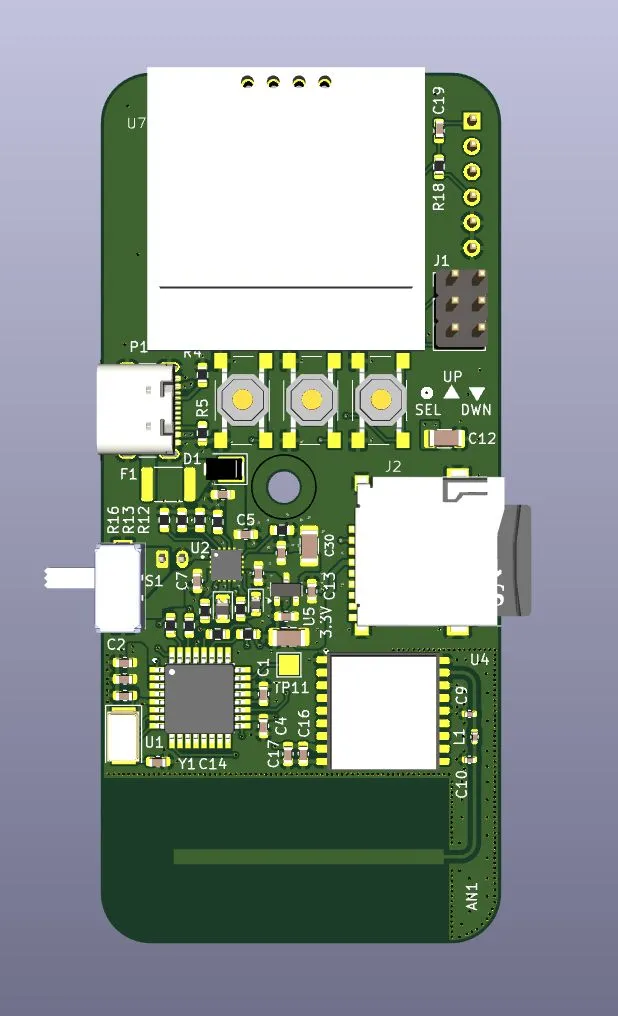
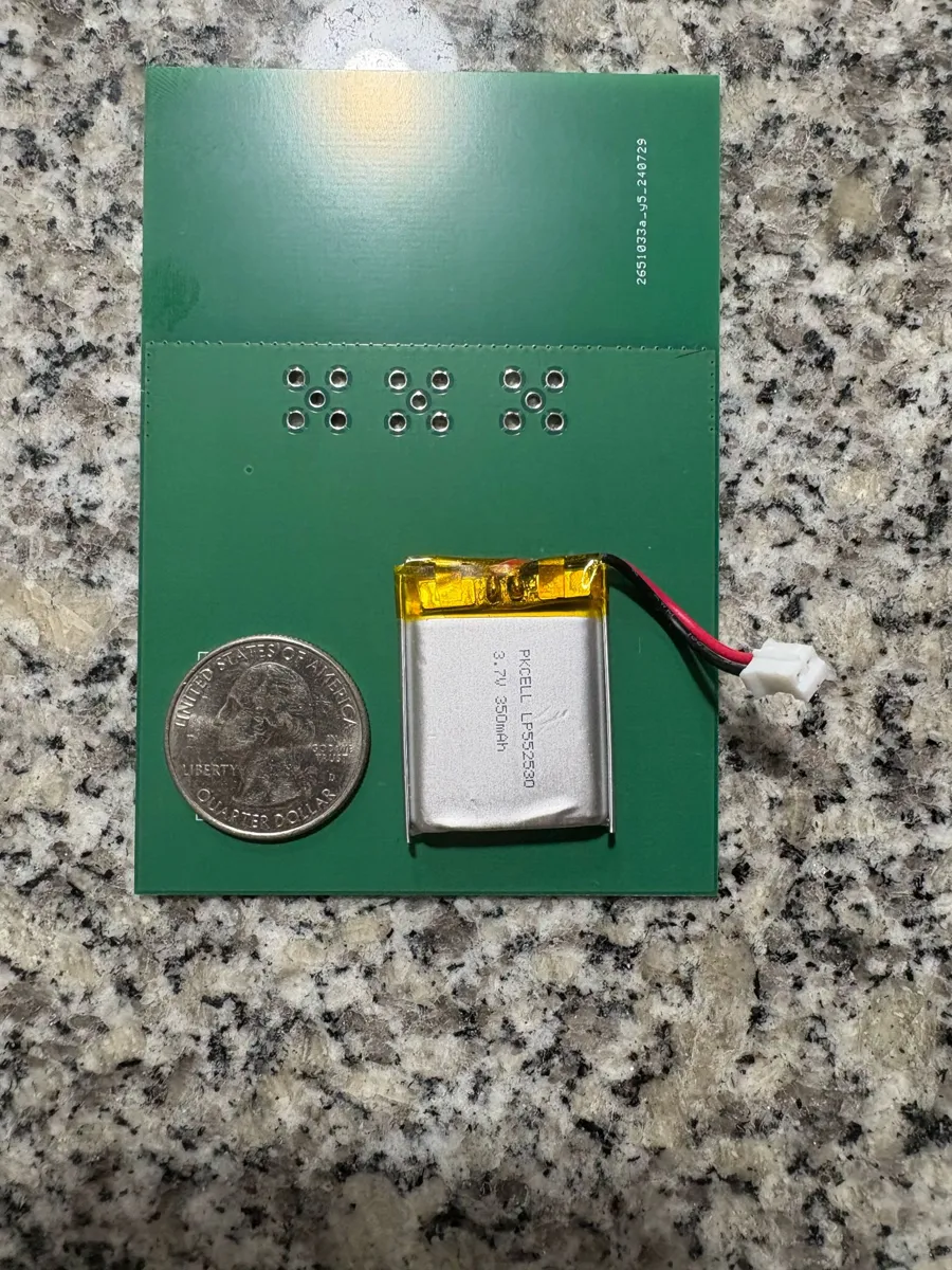
Battery system
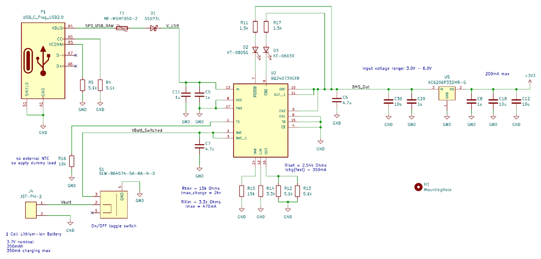
The device runs on a single-cell 350 mAh lithium polymer battery, chosen for the smallest size that still meets the eight-hour minimum battery life. Based on a measured current consumption of 33 mA at 3.7 V, it provides about 10.6 hours of battery life. A TI BQ24073 battery charger and management IC handles precharge, constant-current and constant-voltage charging, and the battery recharges over USB-C. In the schematic the fast-charge current is set to 350 mA, and there is an on/off toggle switch on the battery line.
Schematics
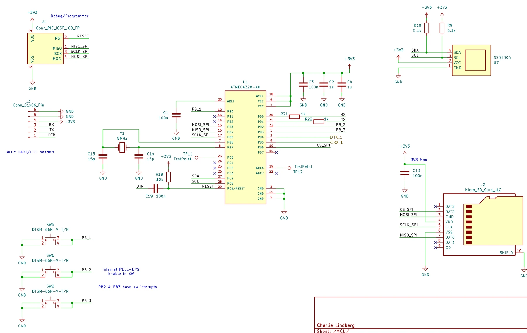
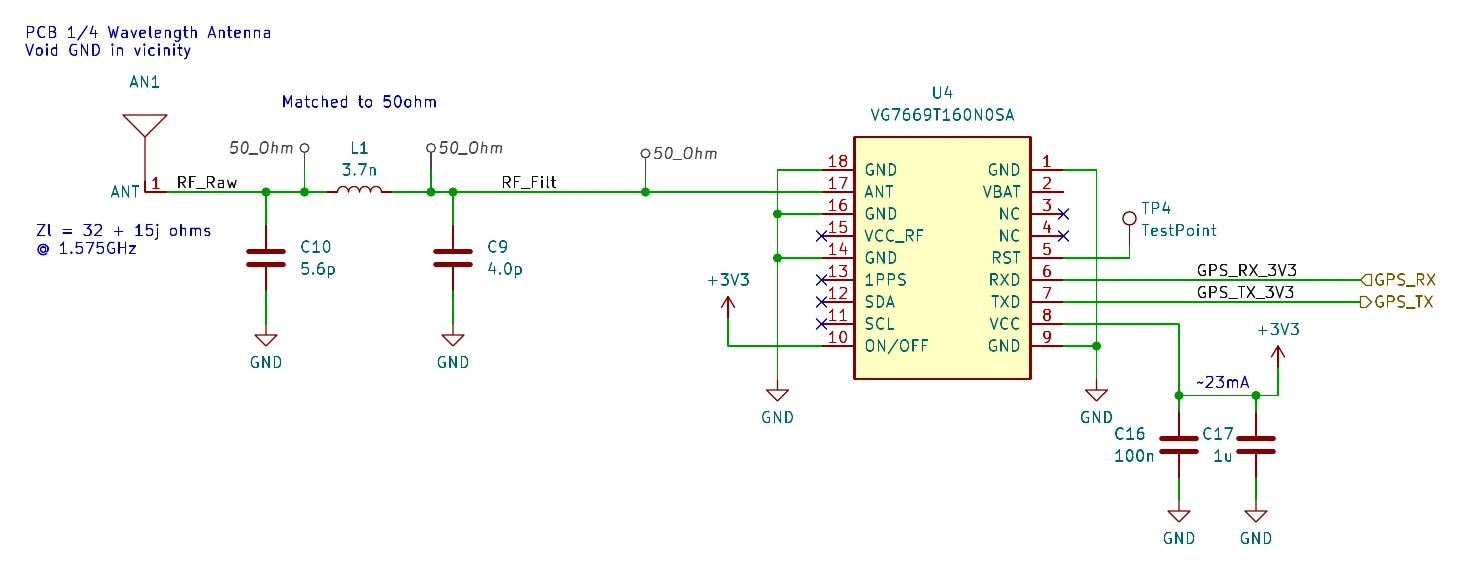
Enclosure
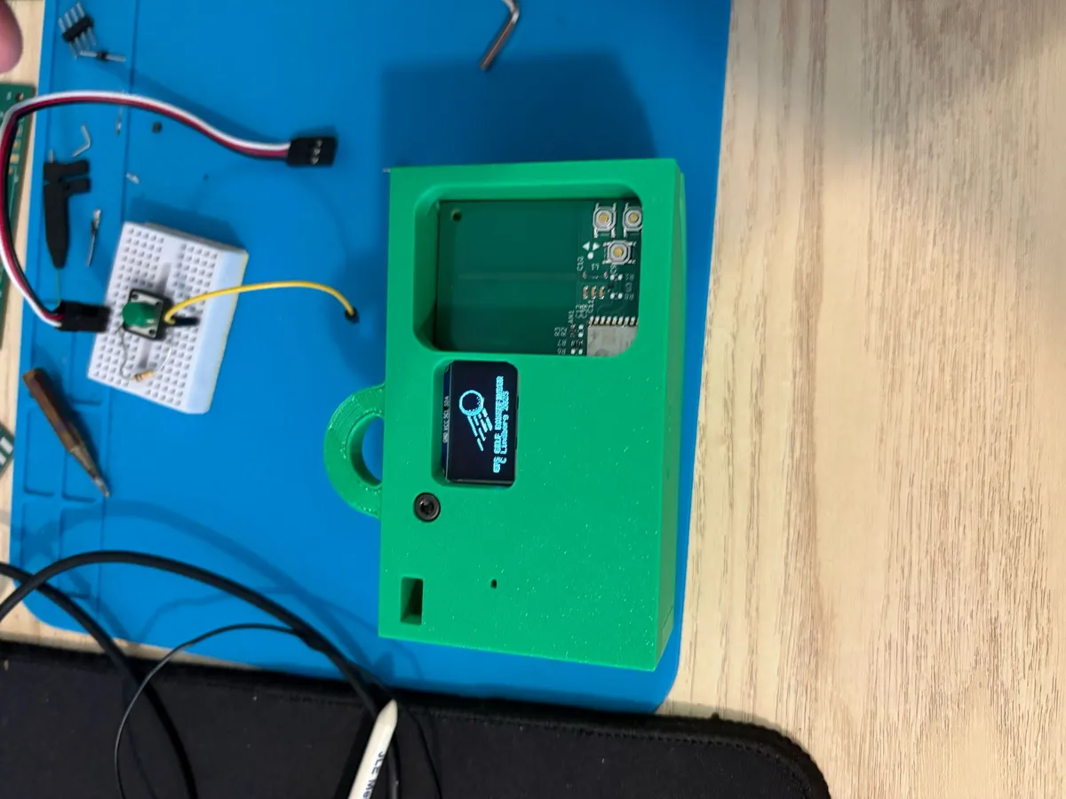
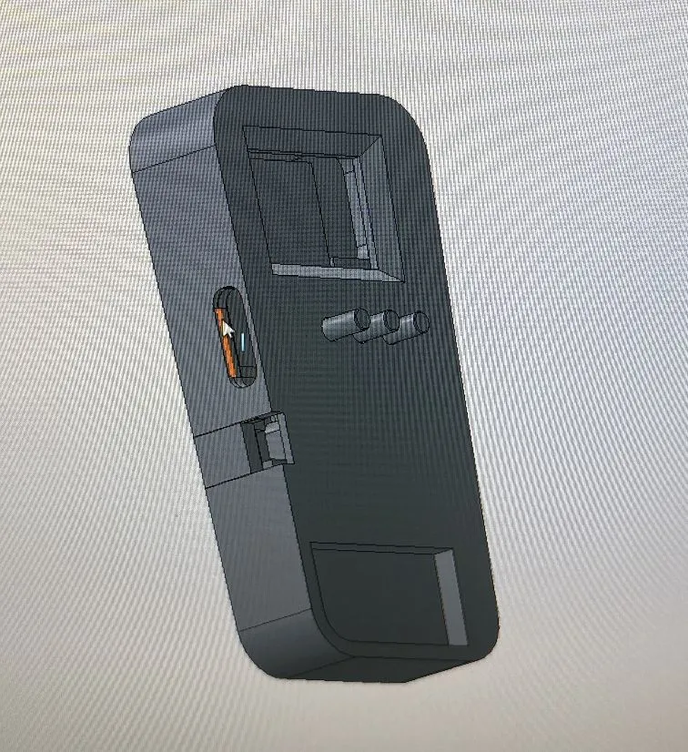
Sam Handel designed the 3D-printed enclosure. There were two different enclosures.
Software
After boot, the microcontroller initializes its systems, then scans a target directory on the SD card to identify the available courses. The user selects a golf course, and the course data is extracted from the corresponding .csv file, where each row is [Hole No.], [Par], [Latitude], [Longitude]. Once the GPS receiver initializes, the distance to the green on hole 1 is displayed, and the user moves to the next hole with the buttons.
Because the distances involved are small (under 1 km), I use an equirectangular projection and the Pythagorean approximation to calculate the distance between two latitude/longitude pairs, with φ as latitude and λ as longitude in radians:
x = Δλ · cos(φm), y = Δφ, d = R · √(x² + y²)
The firmware is written in C++. The firmware source is available here: GPS_RANGEFINDER_FINAL.ino.
Results
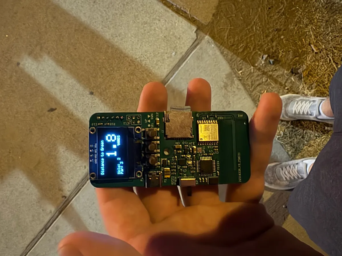
I did initial testing around Austin using points extracted from Google Maps: I would walk to an identified landmark, wait 30 seconds, then record the displayed distance. I also wrote a test program to record the time to a valid GPS fix (the receiver's specification is under 35 seconds), and did additional testing on the course.
| Measurement | Result |
|---|---|
| Distance accuracy (average) | 1.73 yards |
| Cold boot to valid GPS (average) | 42.6 seconds |
| Battery life (from measured 33 mA draw) | ≈ 10.6 hours |
On the course, once the GPS acquired a fix, it gave accurate distances for the whole round.
Cost
The total BoM cost came out to $19.38 per unit at a volume of five units. Non-BoM costs (assembly, shipping, tariffs and tax) added $27.01, for $46.39 per unit in total; those could be driven down at scale.
| Item | Cost per unit |
|---|---|
| PCB | $1.40 |
| SMT BoM | $9.88 |
| Battery | $5.95 |
| Through-hole BoM | $0.46 |
| OLED screen | $1.04 |
| SD card | $0.65 |
| BoM total | $19.38 |
| Assembly (with setup) | $8.23 |
| Shipping | $7.77 |
| Tariffs / tax | $11.01 |
| Total | $46.39 |
The most expensive parts were the LiPo battery ($5.95), the GNSS receiver ($3.85), the MCU ($2.09) and the OLED screen ($1.04). At about $46 per unit in total, the build did not meet the < $25 cost goal. The biggest levers to bring the cost down are a cheaper battery and cheaper PCBA manufacturing.
Lessons learned
Two of the three key design goals were met:
| Goal | Target | Result |
|---|---|---|
| Cost | < $25 | Not met: $46 per unit total |
| Accuracy | < 5 yards | Met: measured 1.73 yards |
| Battery life | 8 hours minimum | Met: more than 10 hours |
Overall I'm generally satisfied with the performance and cost.
What's next
Things to improve in a future revision:
- Power. Lower the MCU clock from 8 MHz to reduce power consumption.
- GPS lock time. Cold boot to a valid GPS fix averaged 42.6 seconds, slower than the receiver's specification of under 35 seconds.
- Cost. The total came in at $46 per unit against the $25 goal; a cheaper battery and cheaper PCBA manufacturing are the biggest levers to get under it.